3D Workspace
Home
Assets
Affiliate Program
Sign up/Log in
?
Upgrade
DCC Bridge
Anonymous1765970573
12-18 04:02
Model Name
lab equipment 3d model
Tags
lab equipment
laboratory instrument
machine
machine realistic
machine rendering
machine rendering realistic
modular
realistic
rendering
rendering realistic
semiconductor
Prompt
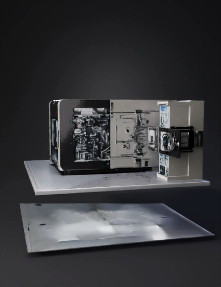
3D DESCRIPTION: PHOTOLITHOGRAPHY TOOL – SEMICONDUCTOR FAB This 3D model represents a state-of-the-art photolithography tool installed inside an ISO Class 1–2 semiconductor cleanroom, designed for advanced wafer patterning at nanometer scales. The tool is shown in a fully assembled operational configuration, highlighting both its external structure and internal functional modules. Overall Structure and Placement The photolithography system is positioned on a vibration-isolated concrete pedestal above a raised cleanroom floor, ensuring nanometer-level stability. The tool footprint is rectangular and elongated, with clear separation between wafer handling, optical exposure, and control systems. Overhead, ULPA-filtered laminar airflow flows vertically downward to maintain ultra-low particle concentration at wafer level. Front-End Wafer Handling Section At the front of the tool, the FOUP (Front Opening Unified Pod) load ports are visible. These load ports interface with the fab’s AMHS (Automated Material Handling System), allowing sealed wafer carriers to dock automatically. Inside this section, robotic wafer transfer arms precisely move individual wafers from the FOUP into the internal processing chambers without human contact. Photoresist Coating Module (Spin Coater) Within the internal chamber, the photoresist spin coater unit is shown. This module dispenses liquid photoresist at the center of the wafer, which then spins at high speed to form a uniform thin film. Surrounding the spinner are chemical exhaust lines, solvent recovery paths, and splash containment walls, all clearly visible in the 3D layout. Soft Bake and Hard Bake Plates Adjacent to the spin coating area are temperature-controlled hot plates used for soft bake and post-exposure bake processes. These plates remove solvents and stabilize the photoresist. The model shows embedded thermal sensors, heating elements, and closed-loop temperature controllers integrated beneath the wafer surface. Exposure Optics and Scanner Stage The core of the tool is the optical exposure module, enclosed within a sealed, light-tight housing. Inside, the projection optics, reticle (mask) stage, and wafer stage are aligned along a precision optical axis. The wafer stage is mounted on magnetically levitated or air-bearing platforms, enabling ultra-fast and ultra-precise scanning motion. The reticle stage is shown above, holding the patterned mask used to transfer circuit designs onto the wafer. Light Source System The model illustrates a deep ultraviolet (DUV) or extreme ultraviolet (EUV) light source, depending on node technology. Light paths are shown traveling through mirrors and lenses before reaching the wafer surface. Shielding panels and purge gas lines protect optical components from contamination. Alignment and Metrology Subsystems Integrated sensors, cameras, and alignment optics are visible around the exposure chamber. These systems ensure sub-nanometer overlay accuracy, aligning each new pattern layer with existing features on the wafer. Real-time feedback systems are represented through control cables and embedded processors. Control Cabinets and Electronics On the side and rear of the tool, electrical cabinets, power distribution units, and control computers are shown. These manage motion control, optics, temperature regulation, and recipe execution. Cable trays route signals cleanly beneath the raised floor and along the tool frame. Utility Interfaces and Sub-Fab Connections Beneath the raised floor, the 3D model reveals chemical supply lines, vacuum exhaust ducts, cooling water pipes, and process gas connections leading to the sub-fab. This separation keeps heat, vibration, and contamination sources away from the cleanroom environment. Cleanroom Integration The tool is fully integrated into the cleanroom layout, with sufficient maintenance clearance zones, operator access panels, and safety interlocks. Overhead ULPA filters ensure continuous downward airflow, while return air grilles in the raised floor maintain pressure balance. Functional Purpose This photolithography tool enables the precise transfer of circuit patterns onto silicon wafers, forming the foundation of modern semiconductor devices. Every visible component in the 3D model emphasizes accuracy, cleanliness, and automation—core requirements for high-yield semiconductor manufacturing.
Detailed Info
Related Models
Enter invite code
Enter invite code to get credits!