View Plans
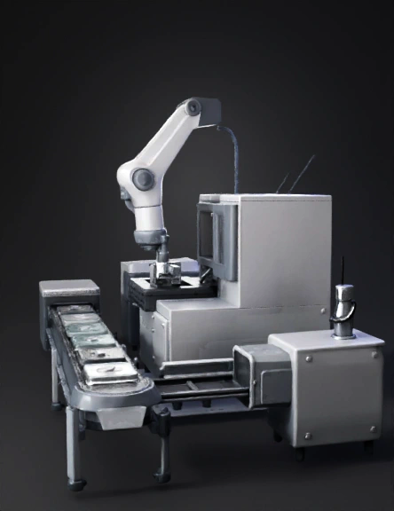
Semiconductor Tool 3d Model: A Detailed 3D Isometric Model Of A Semiconductor Manufacturing Process Setup, In | Tripo AI

semiconductor tool 3d model

Prompt

A detailed 3D isometric model of a semiconductor manufacturing process setup, including a scanner exposure tool, interface module, and post-exposure bake station. The scene shows silicon wafers moving between machines via a robotic arm and conveyor path. Clean industrial environment with white and light grey machines, minimalistic design, smooth surfaces, and realistic proportions. Include labeled sections like "Interface Module", "Scanner Exposure Tool (300mm)", and "Post Exposure Bake (PEB 120°C)". Soft lighting, high-quality textures, and professional engineering visualization style. Centered composition, no background clutter.

4K·PBR·v3.1-20260211

Related Models
3d model: pink heart jewel with white starburst motif and pink central gem3d model: six story modern apartment building with balconies large windows and3d model: witch girl sitting on a carved pumpkin with cat fantasy character wit3d model: carburetor housing gray machined metal with bolt holes and mounting s3d model: pink knitted glove with decorative pattern and teal fingertip accents3d model: green spiked clamp pieces with brown central sphere3d model: cylindrical Philips smart speaker with vertical ribbing black body s3d model: rusted metal crown with arches and fleur de lis accents antique decor3d model: villain character wearing pinstripe suit with glowing orange eyes bla