View Plans
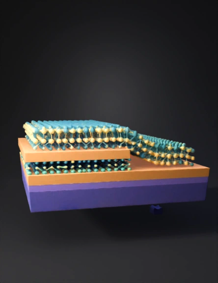
3D Model: Cross section schematic of MoS2 Au hBN SiO2 Si layered semiconductor s
avatarwxk2418009782
01-26 06:45
Model Name

semiconductor stack 3d model

Input
Input image for 3D model generation
Prompt
Related Models
3d model: sculptor figure at workbench with modeling blocks3d model: purple mecha robot with rounded armored limbs and turbine like feet3d model: silver abstract bird like sculpture with smooth curves and sculpted su3d model: capacitor stack with blue and red markings metal blocks mounted on a3d model: stone tower with crenellated battlements and narrow slits built from s3d model: A T rex3d model: two young women portrait with sunglasses and playful expressions3d model: Art nouveau polished brass chess piece knight with embedded gemstones3d model: camera module on blue PCB with gold contact pads and small integrated3d model: ornate long sword with vine engravings along blade and crossguard bla
Enter invite code to get credits!