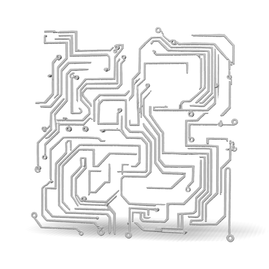
pcb circuit board 3d model
Use the uploaded image as the exact reference. Convert this PCB pattern into a reusable physical stencil/template. Preserve the exact original geometry, proportions, positions, curves, corners, holes, and all circuit-trace shapes. Do NOT redesign, simplify, or add anything. The important change is: remove all filled/solid areas inside and between the circuit lines, making those areas completely empty/open. Keep only the thin solid boundaries and circuit-line structure needed to form the stencil. Every enclosed area should become an open cut-out/negative space, so when the stencil is placed on a sheet of paper, I can draw with a pencil through the open spaces and reproduce the exact pattern. Make it a clean 2D flat stencil, high contrast, with clearly separated open spaces, suitable for 3D-printing as a reusable stencil. No colors, no shading, no texture, no perspective, no background, no artistic changes.
v3.1-20260211


