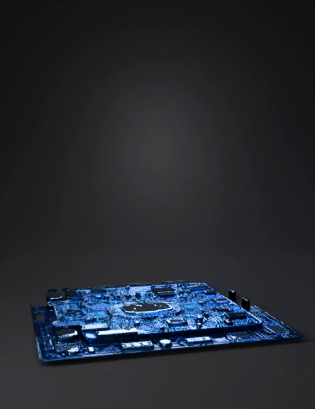
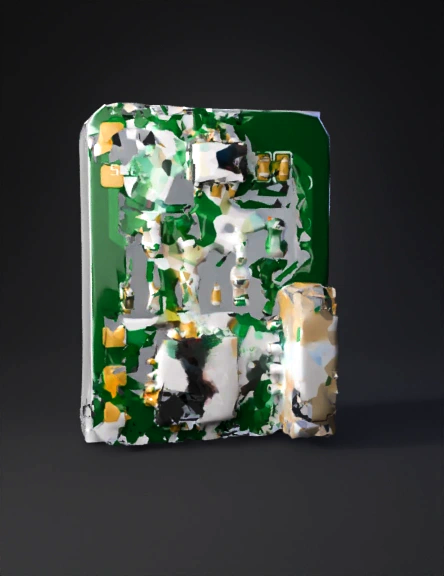
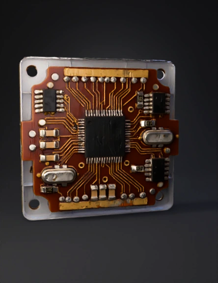
Circuit Board 3D Model
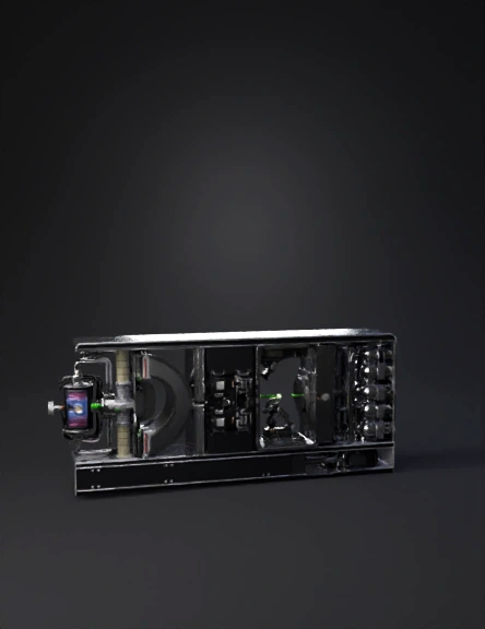
Futuristic Machine 3D Model
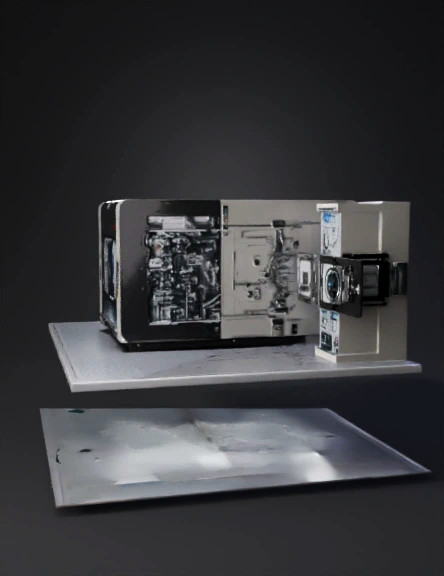
Lab Equipment 3D Model
Momentum Emblem 3D Model
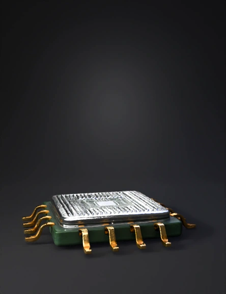
Qfp Microchip 3D Model
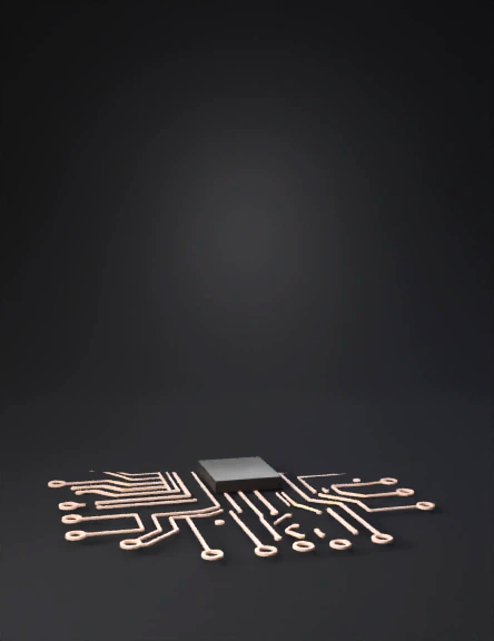
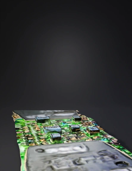
Printed Circuit Board 3D Model
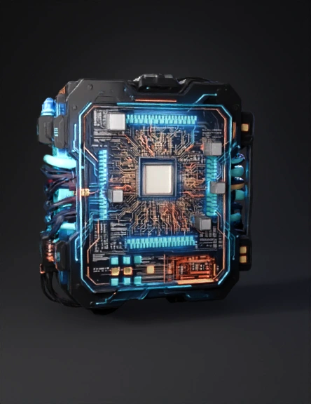
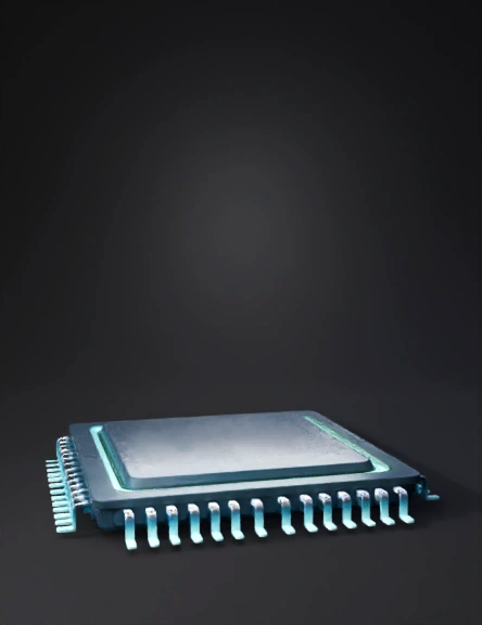
Futuristic Cpu 3D Model
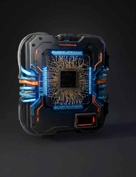
Neon Sci-fi Processor 3D Model
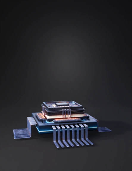
Semiconductor Chip 3D Model
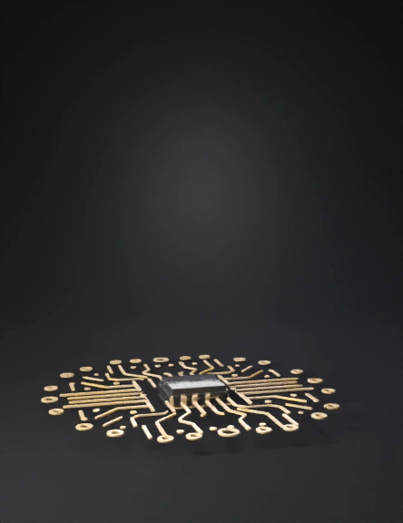
Gold Pcb Microchip 3D Model
Circuit Board 3D Model
Printed Circuit Board 3D Model
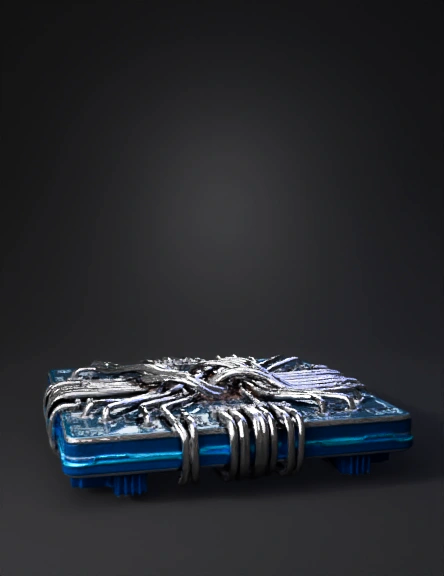
Futuristic Device 3D Model
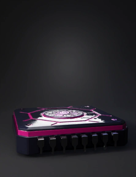
Neon Microchip 3D Model
Futuristic Microchip 3D Model
Circuit Board 3D Model
Microchip 3D Model
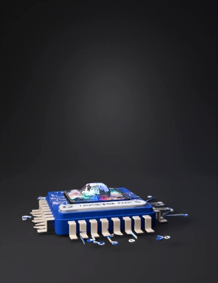
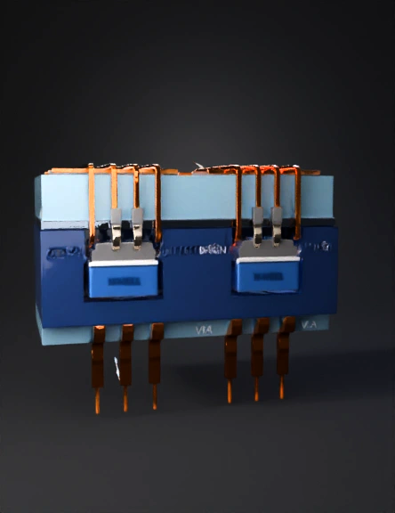
Blue Microchip 3D Model